Assembly
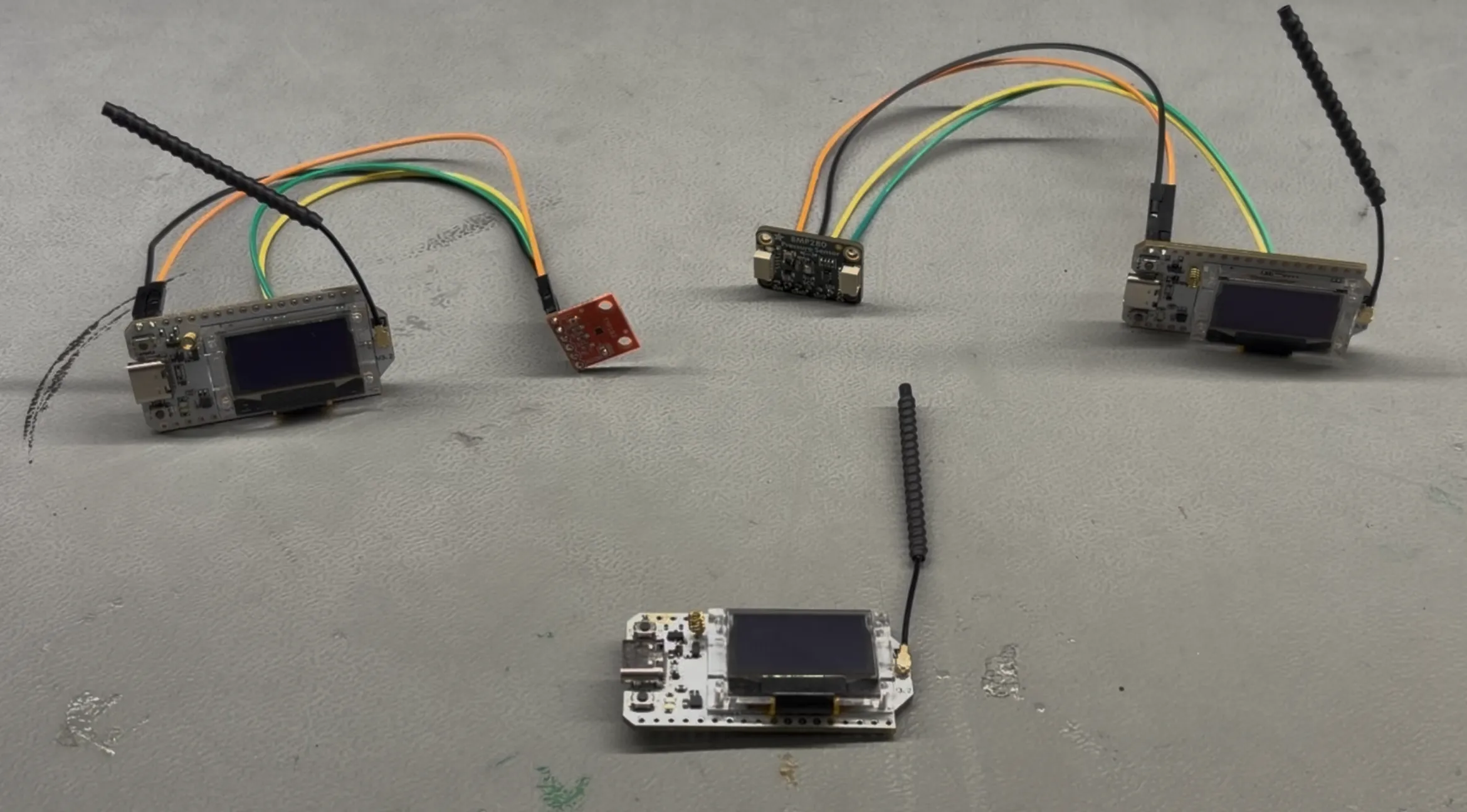
This page walks through the physical assembly of each node type. The receiver node requires no external wiring. The temperature and pressure sensor nodes each require four jumper wire connections between the sensor breakout board and the Heltec board.
Before You Begin
Section titled “Before You Begin”Gather the following for each sensor node:
- 1 Heltec WiFi LoRa 32 V3 board
- 1 sensor breakout board (TMP102 or BMP280)
- 4 jumper wires
- Battery (optional)
Make sure the Heltec board is not connected to USB power while wiring.

Receiver Node
Section titled “Receiver Node”The receiver node uses only the Heltec board with no external wiring. Simply plug it into your computer with a USB-C cable.
The receiver node connects to the monitor application over this USB serial connection. It does not need any sensors because its sole job is to listen for incoming LoRa packets and forward them to the computer.
Temperature Node (TMP102)
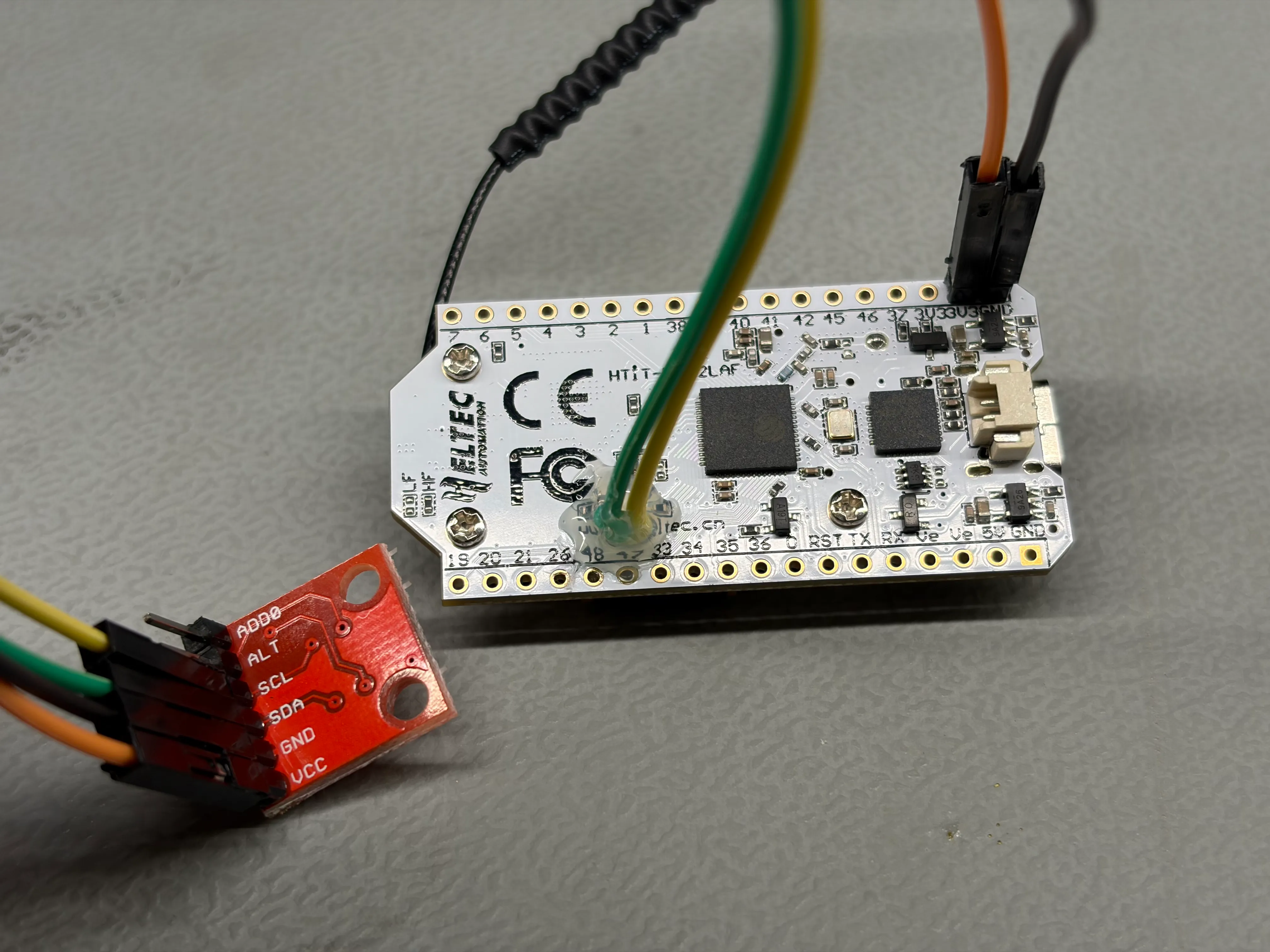
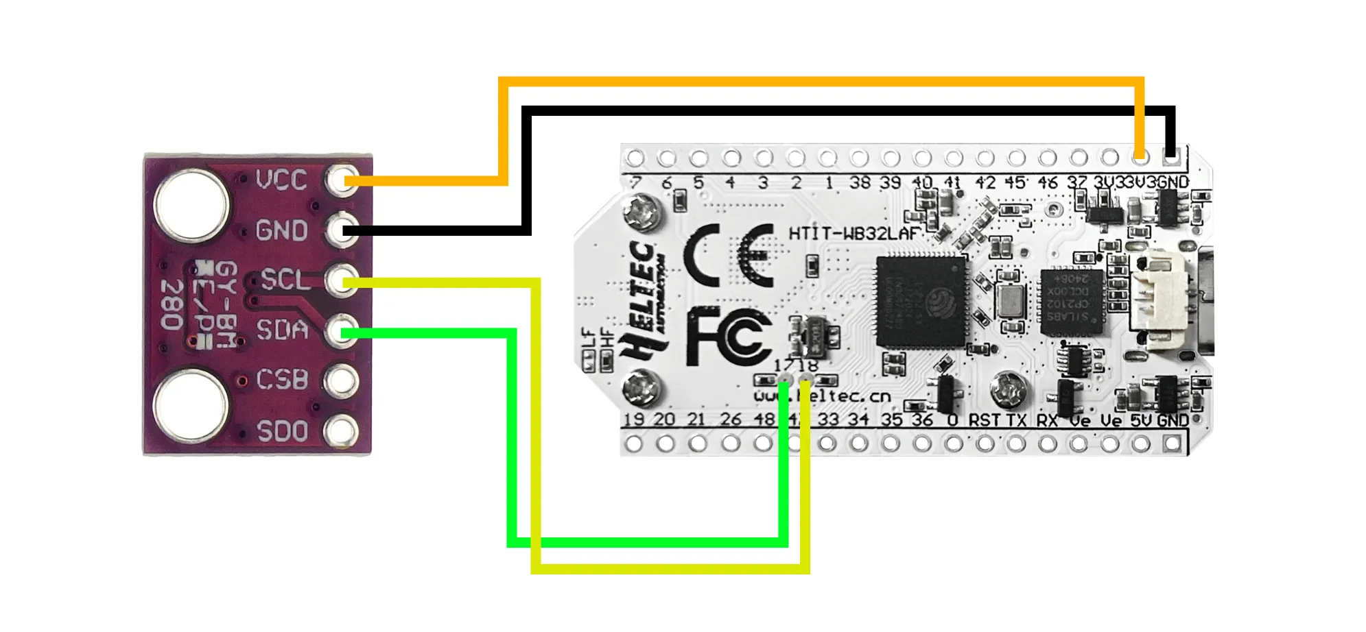
Section titled “Temperature Node (TMP102)”The TMP102 sensor connects to the Heltec board’s I2C bus using four wires. The I2C bus is shared with the onboard OLED display, which is fine because each device has a different address.
Pin Connections
Section titled “Pin Connections”| TMP102 Pin | Heltec V3 Pin | Purpose |
|---|---|---|
| VCC | 3.3V | Power supply |
| GND | GND | Ground |
| SDA | GPIO 17 | I2C data line |
| SCL | GPIO 18 | I2C clock line |
| ADD0 | GND | Sets I2C address to 0x48 |
The ADD0 pin sets the I2C address. Connecting it to GND gives an address of 0x48, which is the default expected by the firmware. If you connect ADD0 to VCC instead, the address changes to 0x49 and you must update TMP102_ADDRESS in config.h.
Assembly Steps
Section titled “Assembly Steps”- Gather the Heltec board and the TMP102 breakout board.
- Solder appropriate headers on both boards.
- Connect a jumper wire from the TMP102 VCC pin to the Heltec 3.3V pin.
- Connect a jumper wire from the TMP102 GND pin to the Heltec GND pin.
- Connect a jumper wire from the TMP102 SDA pin to Heltec GPIO 17.
- Connect a jumper wire from the TMP102 SCL pin to Heltec GPIO 18.

Pressure Node (BMP280)
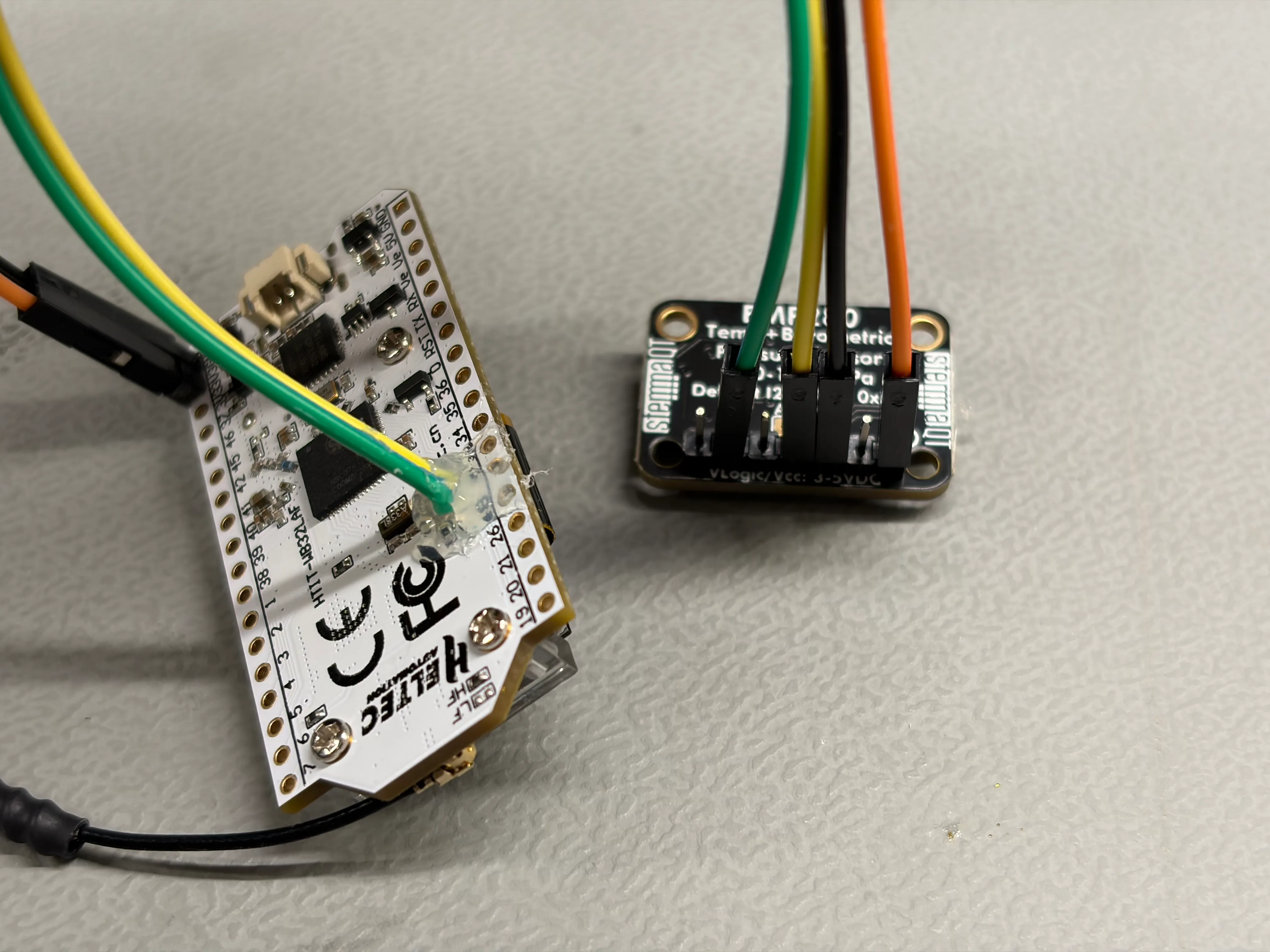
Section titled “Pressure Node (BMP280)”The BMP280 sensor also connects over I2C with the same four data wires, though the pin labels on the breakout board may differ slightly.
Pin Connections
Section titled “Pin Connections”| BMP280 Pin | Heltec V3 Pin | Purpose |
|---|---|---|
| VIN | 3.3V | Power supply |
| GND | GND | Ground |
| SDA | GPIO 17 | I2C data line |
| SCL | GPIO 18 | I2C clock line |
| SDO | GND | Sets I2C address to 0x76 |
The SDO pin sets the I2C address. Connecting it to GND gives an address of 0x76, which is the firmware default. Connecting SDO to VCC changes the address to 0x77 and requires updating BMP280_ADDRESS in config.h.
Assembly Steps
Section titled “Assembly Steps”- Gather the Heltec board and the BMP280 breakout board.
- Solder appropriate headers on both boards.
- Connect a jumper wire from the BMP280 VIN pin to the Heltec 3.3V pin.
- Connect a jumper wire from the BMP280 GND pin to the Heltec GND pin.
- Connect a jumper wire from the BMP280 SDA pin to Heltec GPIO 17.
- Connect a jumper wire from the BMP280 SCL pin to Heltec GPIO 18.
Verifying Your Wiring
Section titled “Verifying Your Wiring”After assembly, you can verify that the sensor is correctly wired before flashing the full firmware. Connect the board to your computer via USB and use the PlatformIO serial monitor or the Arduino IDE’s I2C scanner sketch to check that the sensor responds at the expected address.
Expected I2C addresses for a correctly wired node:
| Device | Address |
|---|---|
| SSD1306 OLED (onboard) | 0x3C |
| TMP102 (if attached) | 0x48 |
| BMP280 (if attached) | 0x76 |
If the sensor does not appear at the expected address, double-check your wiring — particularly that SDA and SCL are not swapped and that the address-select pin (ADD0 or SDO) is connected to GND.
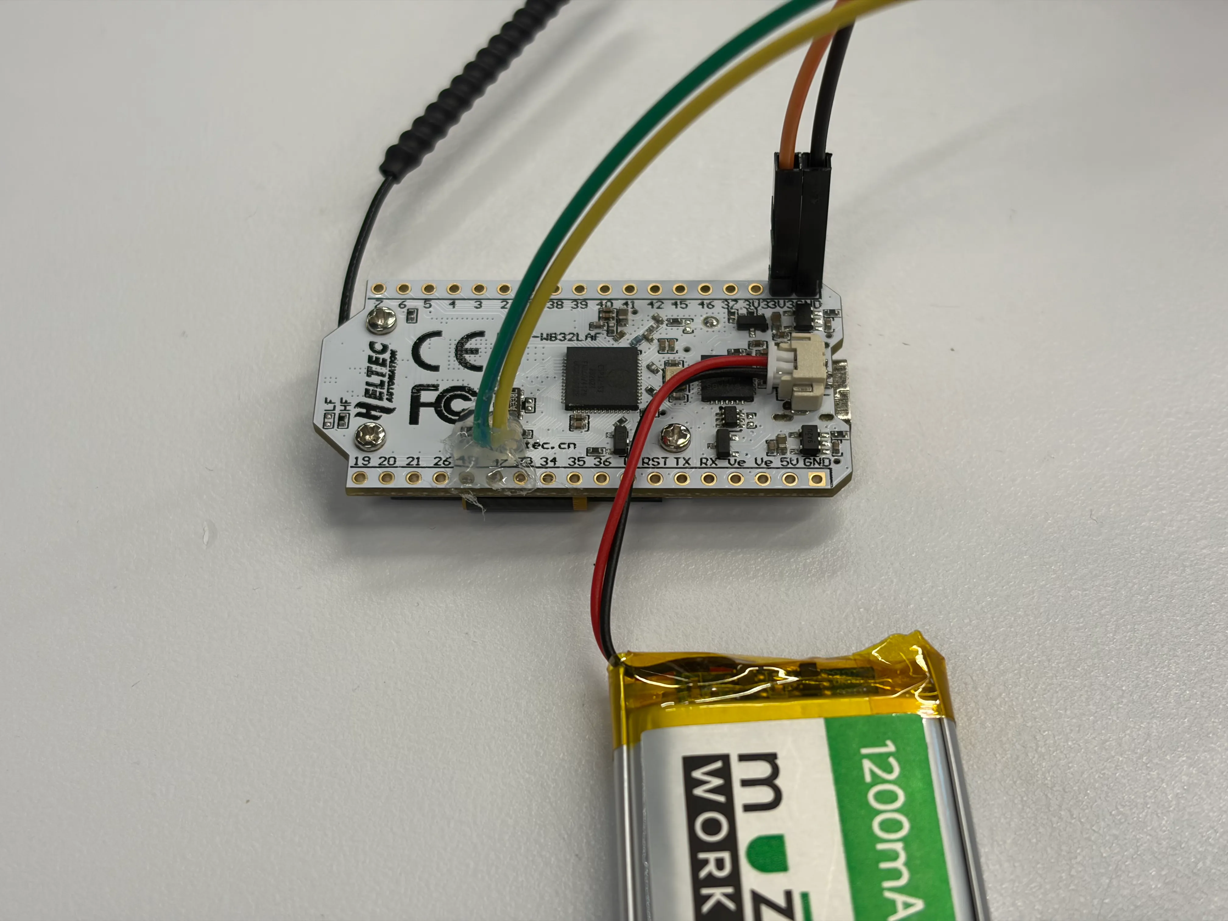
Battery
Section titled “Battery”If you choose to have a battery for your nodes, you can now connect it. The Heltec V3 board makes using a battery super easy. I recommend connecting a battery to just the sensor nodes, since the receiver node will get power over USB from the monitoring computer.
- Keep wires short. Shorter I2C wires are more reliable, especially if you later increase the I2C clock speed.
- Secure the breadboard. The Heltec board can wiggle loose from a breadboard during handling. Press it in firmly or use a dab of mounting tape on the back.
- Label your nodes. If you are building multiple nodes, put a small sticker or tape label on each board indicating its role (Receiver, Temperature, Pressure). This helps when it is time to flash each board with the correct firmware configuration.
- I2C pins are on the back. The I2C pins are in a tricky location, and can’t have pin headers soldered to them. You’ll need to strip the end of two jumper cables and solder directly to the pads. Be careful — they’re small!
Next Step
Section titled “Next Step”With your hardware assembled, head to the Firmware Overview to understand the software that runs on each node.